
 Kontakt
 Kako kupovati
Dostava
Savjetnik za kupnju
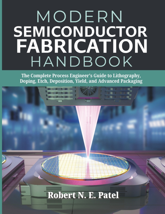
Modern Semiconductor Fabrication Handbook
The Complete Process Engineer's Guide to Lithography, Doping, Etch, Deposition, Yield, and Advanced Packaging
 Engleski
 265 b
265 b
 Novo
Novo
Do 30 dana za povrat

The gap between solid-state physics and a working fab is where careers either take off or stall out.
Most engineers arrive at their first fab role knowing the equations but not the judgment. You can derive a threshold voltage, but you cannot yet explain why splitting a die into chiplets does not automatically raise yield, or why wide metal lines take the brunt of polishing damage during CMP. Vendor manuals give you steps without reasoning, and academic texts give you theory without constraints. Neither one prepares you for the moment a process drifts and you are the one expected to diagnose why.
Modern Semiconductor Fabrication Handbook was built to close that exact gap, and it does so on real industrial terms, not textbook ideals.
Who This Book Is Built ForThis handbook was written for the process and process integration engineer who needs to reason backward from a device target to a manufacturable specification, not just follow a recipe someone else wrote. It speaks equally to the yield optimization specialist who lives inside defect density arithmetic and cost-per-good-die decisions, and to the graduate student stepping out of coursework into an advanced manufacturing role for the first time, where the questions suddenly stop being theoretical. Design engineers will find it useful too, since it explains the physical origin of the layout rules they are told to follow but rarely told to understand. Even technical managers who never touch a wafer benefit from it, because the book lays out, in plain quantitative terms, what a complex fabrication decision actually costs and why.
How This Handbook Works
Every chapter is designed to build engineering judgment, not passive familiarity.
- Build from first principles: Follow the governing physics behind semiconductor materials, devices, thermal processing, vacuum systems, patterning, deposition, etching, interconnects, packaging, and metrology.
- Work through the numbers: Use detailed worked examples to connect equations with practical calculations involving oxidation, diffusion, implantation, lithography, vacuum, process control, and yield.
- Understand model limits: Learn where standard models apply, where assumptions begin to fail, and why the boundary of validity matters in real manufacturing decisions.
- Diagnose with purpose: Troubleshooting sections guide you through common process and equipment faults, helping you distinguish between likely causes rather than relying on vague trial and error.
- Reinforce what matters: Chapter summaries, key takeaways, quick reviews, practice questions, and a comprehensive abbreviation guide help make complex material easier to revisit and apply.
- Yield economics: defect density, die area, and the cost arithmetic behind every architectural decision
- Device fundamentals: carrier concentration, depletion width, and the physics that sets your process targets
- Contamination control: particulate standards, deposition velocity, and killer defect size in cleanroom design
- Front End of Line: transistor formation from shallow trench isolation through gate-all-around and strain engineering
- Lithography and patterning: Rayleigh limits, EUV stochastics, multi-patterning economics, and overlay budgets
- Back End of Line: copper dual damascene, low-k dielectrics, CMP mechanics, and backside power delivery
- Advanced packaging: the yield and thermal logic behind chiplet disaggregation and hybrid bonding
This handbook helps you build the foundation to understand the process, investigate the causes, and make better-informed engineering decisions.
Add Modern Semiconductor Fabrication Handbook to your engineering library today.


Informacije o knjizi
Engleski

Poklonite ovu knjigu još danas
To je jednostavno
1 Dodajte knjigu u košaricu i odaberite isporuku kao poklon 2 Zauzvrat ćemo vam poslati kupon 3 Knjiga dolazi na adresu poklonoprimcaDobar dan! Ja sam Libroamiko, vaš književni savjetnik.
Kako vam mogu pomoći?